Our Location
House no 99 , second floor , Block H-1 , sector 11 , Rohini , New Delhi , 110085 , INDIA

House no 99 , second floor , Block H-1 , sector 11 , Rohini , New Delhi , 110085 , INDIA
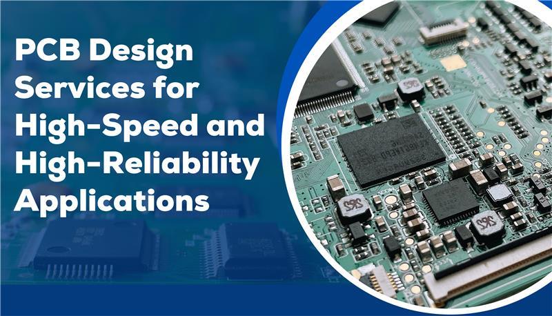
Printed Circuit Boards (PCB) serve as the backbone of electronics systems. It permits seamless communication among electronic components and provides mechanical rigidity and electrical performance.
With applications requiring high-speed data processing, miniaturized electronics, and mission-critical applications becoming more common in industries. Due to this need for quicker and reliable high-speed PCB design is on the rise.
Whether the job at hand is in telecommunications or aerospace, medical devices or automotive electronics, PCB designs today are being asked to hit rigorous performance, durability and compliance benchmarks.
High Performance PCB Design is not just about go-faster, it’s understanding how to make signals travel faster and what will limit them. It’s everything from the physics of materials used up through dimensions and signal integrity.
Similarly, the high-reliable design methodology tends to deal with lifetime performance as well as environmental immunity and fault tolerance. This blog offers the key fundamentals to PCB design services for high speed / high reliability applications: what you need to know before getting started, how easy it is to implement them and benefits of doing so.
PCB design deals with how to handle signals at higher frequencies (typically in the GHz ranges). Applications in which this product is used: High-speed networking equipment, Data rate sensitive electronics, such as computer peripherals, Data center Broadband, telecom, Industrial automation systems, and Advanced computing devices.
Electrical signals no longer behave as currents, but rather as electromagnetic waves There traditional PCB design methodologies fall short at these frequency levels.
Professional PCB design services for high speed application generally encompass schematic capture, controlled impedance routing, high-speed interface design (DDR, PCIe, USB 3.0/2.0/1.x, HDMI and HS Ethernet) and full simulation.
They use sophisticated EDA tools to model the behavior of signals, predict losses and identify problems with their design early in its development cycle. This preemptive process minimizes revision costs and guarantees top performance from the initial prototype.
Signal integrity (SI) and power integrity (PI) are the key issues about high speed PCB designs. Weak signal integrity can lead to loss of data, problems with timing and crosstalk, electromagnetic interference (EMI), while poor power integrity may bring voltage droops, noise and system instability.
In order to preserve signal integrity, trace impedance, length matching termination types and routing topology are managed carefully by PCB designers.
Differential pair routing, controlled impedance lines and spacing are critical factors in order to minimize reflections and noise. Power integrity, meanwhile, is concerned with delivering noise free and stable power throughout the PCB. This includes good positioning of decoupling capacitors, low-inductance power planes and an optimized PDN.
SI/PI simulations are utilized in advanced high reliability PCB design to provide insight into system behavior in real world circumstances. These simulations are useful to locate potential bottlenecks, and designers may optimize layouts for better performance and reliability.
The power supply line or main traces do exactly what the name suggests, it powers the entire circuit and it can be considered as the system’s bloodstream where it feeds current to all “life” points in the product, each device component tends to be powered from the main source.
These design guidelines offer a disciplined approach to designing PCBs that are reliable and resistant to failure over time – abilities that will be tested as we move into Industry 4.0 and beyond. Critical design methodologies include placement of components, planning for thermal and grounding.
High power dissipation components are spaced to allow effective heat transfer and sensitive parts are placed away from noise sources. In addition, redundant routing paths, wider traces in critical signals and strengthened vias are also resorted by designers to improve both mechanical strength and electrical integrity.
Grounding strategies like solid ground planes, star grounding and controlled return paths also alleviates noise and enhances overall system integrity. These practices are critical in such industries as aerospace, defense and medical electronics where system failure can have catastrophic consequences.
Choosing the right materials and designing of PCB stack-up are essential in attaining high-speed performance and long-term reliability. The choice of laminate affects Ioss, thermal and mechanical matters in high-speed PCB design. Although standard FR-4 materials suffice for most applications, high speed designs commonly necessitate advanced materials with lower dielectric constants and dissipation factors.
Designers utilize materials including high frequency laminates, low-loss prepregs and proprietary copper foils in their high speed PCB designs. Stack-up planning is where we decide the total layer count, relationship between signals and planes, impedance-controlled structures etc. A properly implemented stack-up offers consistent signal integrity, reduced EMI and effective power distribution.
Professional PCB Design services work closely with manufacturers during the stack-up planning to assure that design intent is compatible with fabrication process. This effort allows to avoid manufacturing problems and guarantee that the design satisfies performance and reliability targets.
Design for Manufacturing (DFM) and Design for Assembly (DFA) play a big part in offering quality PCB design services. The best design in the world is worthless if it cannot be produced of effectively and assembled right. As in the case with DFM/DFA, however, checks for tolerances based on manufacturing processes (e.g., the tolerance between PCB layout-matching drills and tools) are made.
This includes trace widths and spaces, via sizes, solder mask openings and component footprints. They also factor in the needs of automated assembly, thermal profiles for soldering and inspection access. By taking into account these variables at the beginning of the design process, PCB design services minimize production risks, optimize yield and reduce manufacturing costs.
In high reliability applications DFM/DFA also includes adherence to industry standards such as IPC, ISO and industry specific regulation. This guarantees the uniform quality and durability through production runs.
Verification and validation are crucial phases in verifying that high-speed PCB design will perform as intended. High-Speed High-Reliability PCB Design Services Follow Rigorous Testing Procedures Throughout the Process. Electrical testing, signal integrity verification, thermal analysis and environmental stress tests are part of this.
Prototype tests enable to validate the design assumptions and highlight practical problems which may not be reached in simulations. Time domain reflectometry (TDR), eye diagram analysis, and impedance measurements are also regularly used to confirm high-speed signal integrity. We may perform accelerated life tests, vibration testing and thermal cycling as part of reliability assurance of the product.
End users are confident in the readiness for deployment since there is extensive documentation and test reports. These validation activities substantially minimize the possibility for field failures, leading to increase in product reliability.
To meet the rigorous demands for high-speed and reliability, PCB designs must incorporate a delicate balance of engineering experience, powerful design tools and industry best practices.
The high-quality designs that are made through professional PCB design services manage to live up to the high expectations of today’s ever evolving applications.
An investment in experienced PCB design capability will lead to higher performance and reliability and expedite time-to-market while mitigating long-term running risks. For those seeking to build groundbreaking electronics, great PCB design is not an option it’s a strategic requirement.