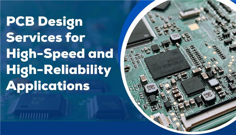
Printed Circuit Boards (PCB) serve as the backbone of electronics systems. They permit seamless communication among electronic components and provide mechanical rigidity and electrical performance.
With applications requiring high-speed data processing, miniaturized electronics, and mission-critical performance becoming more common, the need for high-speed PCB design is on the rise. Whether the job is in telecommunications, aerospace, medical devices or automotive electronics, PCB designs today must hit rigorous performance, durability and compliance benchmarks.
High Speed PCB Design. An Introduction
High-speed PCB design deals with how to handle signals at higher frequencies (typically in the GHz range). Applications include high-speed networking equipment, data-rate-sensitive electronics, data centre broadband, telecom, industrial automation systems, and advanced computing devices.
At these frequency levels, electrical signals behave as electromagnetic waves, this is where traditional PCB design methodologies fall short. Professional PCB design services for high-speed applications encompass schematic capture, controlled impedance routing, high-speed interface design (DDR, PCIe, USB 3.0, HDMI, and HS Ethernet) and full simulation.
Signal Integrity and Power Integrity Considerations
Signal integrity (SI) and power integrity (PI) are the key issues in high-speed PCB designs. Weak signal integrity can lead to loss of data, timing problems, crosstalk and electromagnetic interference (EMI), while poor power integrity may bring voltage droops, noise and system instability.
To preserve signal integrity, trace impedance, length matching, termination types and routing topology are managed carefully. Differential pair routing, controlled impedance lines and spacing are critical to minimise reflections and noise. Power integrity is concerned with delivering noise-free and stable power throughout the PCB, this includes careful positioning of decoupling capacitors, low-inductance power planes and an optimised PDN.
PCB Layout Techniques for High-Reliability Designs
High-reliability PCB designs follow a disciplined approach covering component placement, thermal planning and grounding strategy. High power dissipation components are spaced to allow effective heat transfer, and sensitive parts are placed away from noise sources.
Designers also use redundant routing paths, wider traces on critical signals and reinforced vias to improve both mechanical strength and electrical integrity. Grounding strategies like solid ground planes, star grounding and controlled return paths reduce noise and enhance overall system integrity, critical in aerospace, defence and medical electronics where failure can have catastrophic consequences.
Material Selection and Stack-Up Planning
Choosing the right materials and designing the PCB stack-up are essential to attaining high-speed performance and long-term reliability. Although standard FR-4 suffices for most applications, high-speed designs commonly require advanced materials with lower dielectric constants and dissipation factors, including high-frequency laminates, low-loss prepregs and specialised copper foils.
Stack-up planning determines the total layer count, the relationship between signals and planes, and impedance-controlled structures. A properly implemented stack-up offers consistent signal integrity, reduced EMI and effective power distribution.
Design for Manufacturing and Assembly (DFM/DFA)
The best design in the world is worthless if it cannot be produced effectively. DFM/DFA checks include tolerances based on manufacturing processes, trace widths and spaces, via sizes, solder mask openings and component footprints. In high-reliability applications, DFM/DFA also includes adherence to industry standards such as IPC, ISO and industry-specific regulations.
Testing, Validation, and Reliability Assurance
Verification and validation are crucial phases in confirming that a high-speed PCB design will perform as intended. Electrical testing, signal integrity verification, thermal analysis and environmental stress tests are all part of the process. Time domain reflectometry (TDR), eye diagram analysis and impedance measurements confirm high-speed signal integrity.
To meet the rigorous demands for high-speed and reliability, PCB designs must incorporate a balance of engineering experience, powerful design tools and industry best practices. An investment in experienced PCB design capability leads to higher performance and reliability, expedites time-to-market, and mitigates long-term risks.
Have a project in mind?
Talk to our embedded design experts for a free consultation.
Get Free Consultation